


Inner Layer Process
(I): Panel Cutting and Pre-Treatment
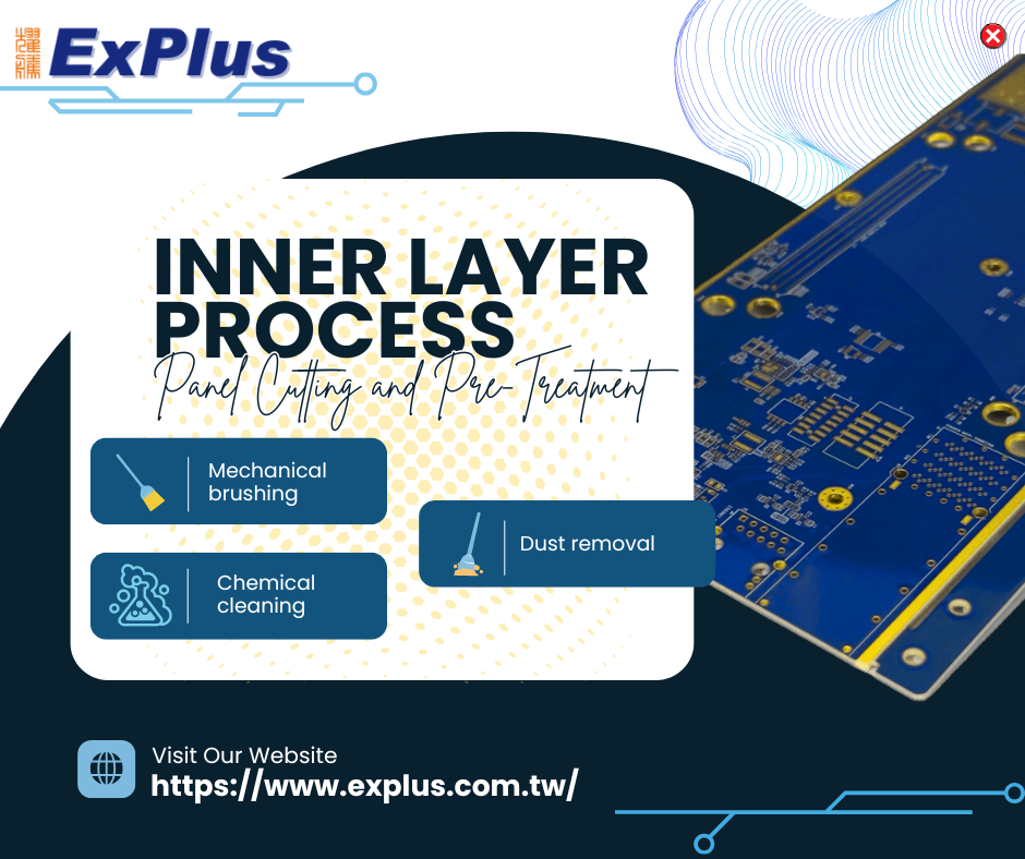
The first step in the inner layer PCB manufacturing process begins with large copper-clad laminates. Since the original panels are typically oversized, they must first be cut into appropriate working dimensions according to production requirements using a cutting machine.
Following cutting, the panels undergo pre-treatment, a critical process designed to ensure that the copper surface is clean, roughened, and uniform. Pre-treatment generally consists of three main stages: mechanical brushing, chemical cleaning, and high-pressure dust removal.
- Mechanical brushing removes the oxide layer and increases surface roughness.
- Chemical cleaning eliminates oil, fingerprints, or other contaminants.
- Dust removal ensures that fine particles are completely cleared from the surface.
Poor surface preparation may lead to defects such as photoresist peeling, short circuits, or incomplete circuitry during the exposure and etching stages. Although pre-treatment may appear simple, it is in fact a key determinant of product quality and a vital part of the entire PCB fabrication process.