- Home
- MCPCB
MCPCB Manufacturing Process

- 01. Material
- 02. Drilling
- 03. Dry Film Image Transfer
- 04. Solder Mask
- 05. Routing
- 06. V-Cut
- 07. Test
- 08. HiPot
MCPCB stands for Metal core printed circuit board, incorporates a metal material as its base.
The basic structure of MCPCB is composed of the following parts:
● Solder mask
● Circuit layer
● Copper layer
● Dielectric layer - prepreg(PP) / fiberglass(FR-4)
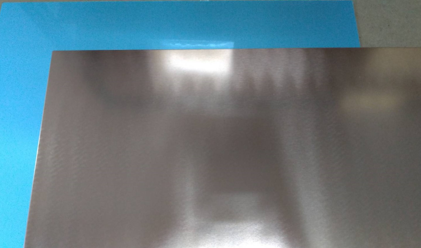
● Matel base - Aluminum alloy 5052 
Use CNC drilling machine to drill holes, which for connecting conductor from layer to layer and mounting components.
Processing holes such as parts holes, fixed holes, and via holes according customer’s design, and provide positioning holes required for subsequent processes. The drilling machine is computer-controlled. The operator set up the drill program. High speed drilling ensures clean hole walls to provide a secure base for good plating on the hole walls.
Drilling is a slow process as each hole must be drilled individually. We can drill holes down to 8 mil in diameter. Drill change is fully automatic. The machine selects the correct drill to use from the drill rack, and then loads it into the drill head.
Make wire traces on the outer layer of the copper-plated board.
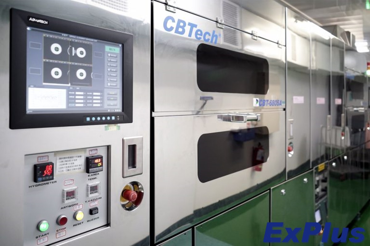
Cover the surface of the board with a layer of organic film that is optically active, and after exposure, transfer the pattern of the outer film to the board surface. And thicken the outer layer circuit by second electroplating.

Cover the PCB with insulating resin to protect the tracks of the outer layer from oxidation and short circuits.
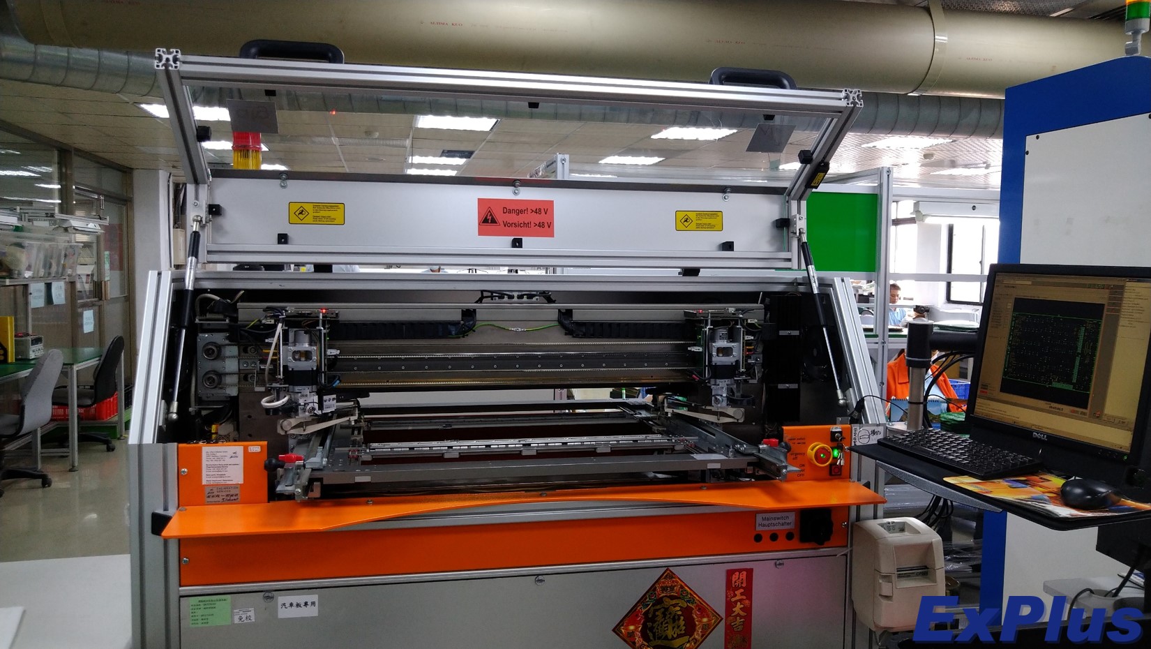
Soldermask is a protective layer of liquid photo imageable lacquer applied on the top and bottom side of a PCB. The function of the soldermask is to protect the copper from oxidation, environmental influences like dust and other contaminations that may create circuit shorts in the long run.

A CNC milling machine is used to form the PCB according to the required design contour.
Routing or milling is a technique performed on a CNC machine with a routing tool. Milling is used to form the contour of the PCB at the very end of the production process. For this, we use a computer-controlled milling machine. First the machine mills out any small slots or internal cut-outs. The cutter follows the path defined in the original tool file and mills around each PCB. The brush around the milling head ensures that all the dust produced is collected by the vacuum system.
A cutting line is formed on the surface of the PCB to make it easier to depanelized.
V-cut also named as V-Scoring or V-grooving, it is the final manufacturing stage of PCBs. It is cutting a “v” groove on the top and bottom of a PCB while leaving a minimum amount of material, so that a individual PCB can be easily separated from the production panel.
Conduct electrical tests and other necessary tests to ensure the quality of the circuit board.
ExPlus conducts 100% electrical tests on circuit boards before shipping to the costumer. We also provide Hipot test to meet the requirement of customers. Our PCB test systems include:
● The flying probe testers, which are suitable for testing small batches and highly complex PCBs.
● Universal grid testers, which require the use of a separate test fixture, are well suited for testing bulk-manufactured PCBs.

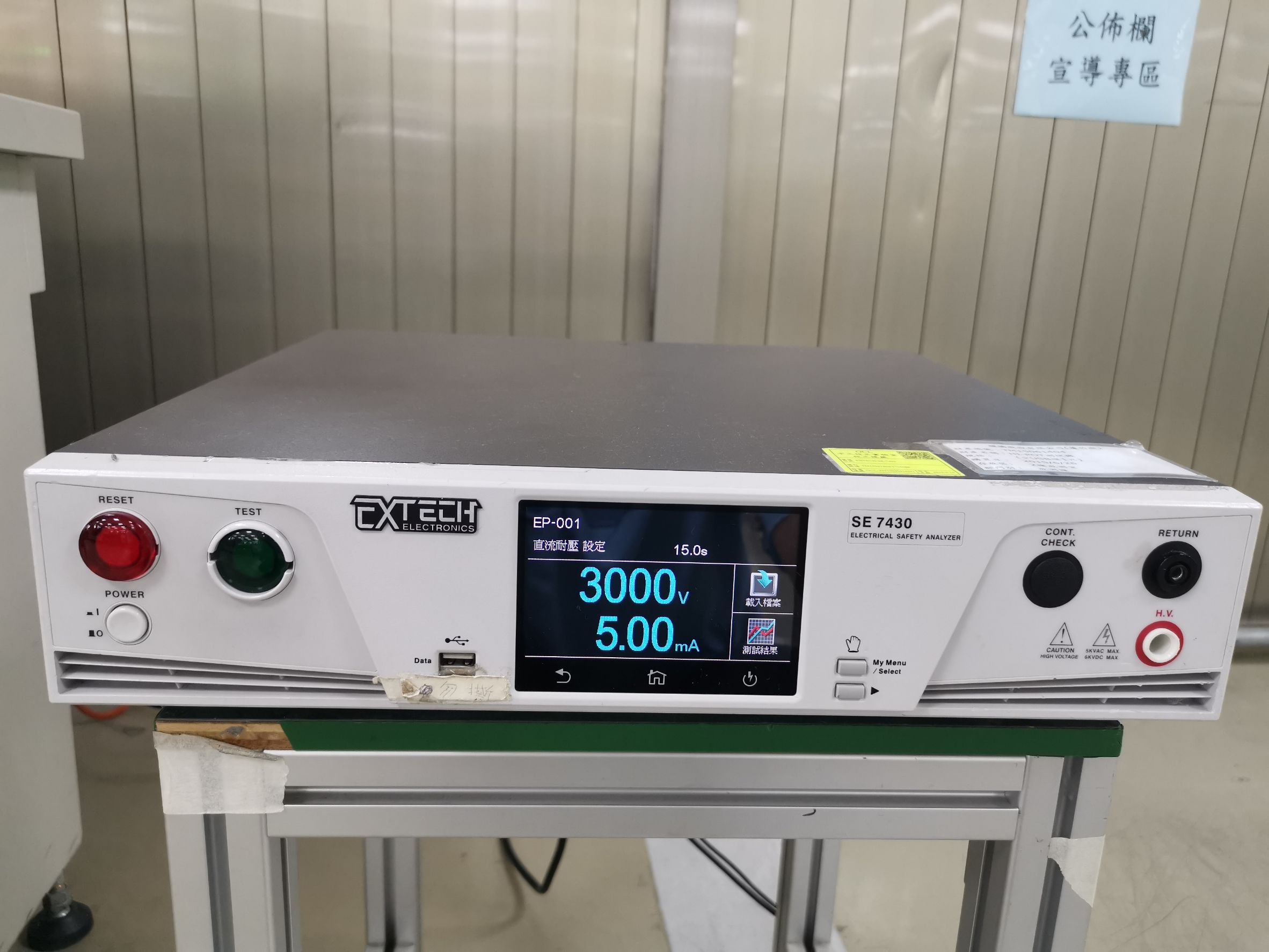
HiPot test, also known as dielectirc withstand voltage test.
It is a non-destructive reliability test that can measure the “breakdown voltage” and “insulation resistance” of PCBs to detect whether the electrical safety of PCBs meets the characteristics and insulation performance requirements.
The HiPot test can also detect potential defects in PCBs, such as:
● The insulating effect of the insulating material is not good.
● There are pinholes on the insulator.
● Insufficient electrical clearance between components.
● The insulator is squeezed and broken.


