¿Cuales son los pasos del proceso de construir capa interior?
The pre-treatment that we discussed in last article was mainly to enhance the adhesion to help following inner layer process.
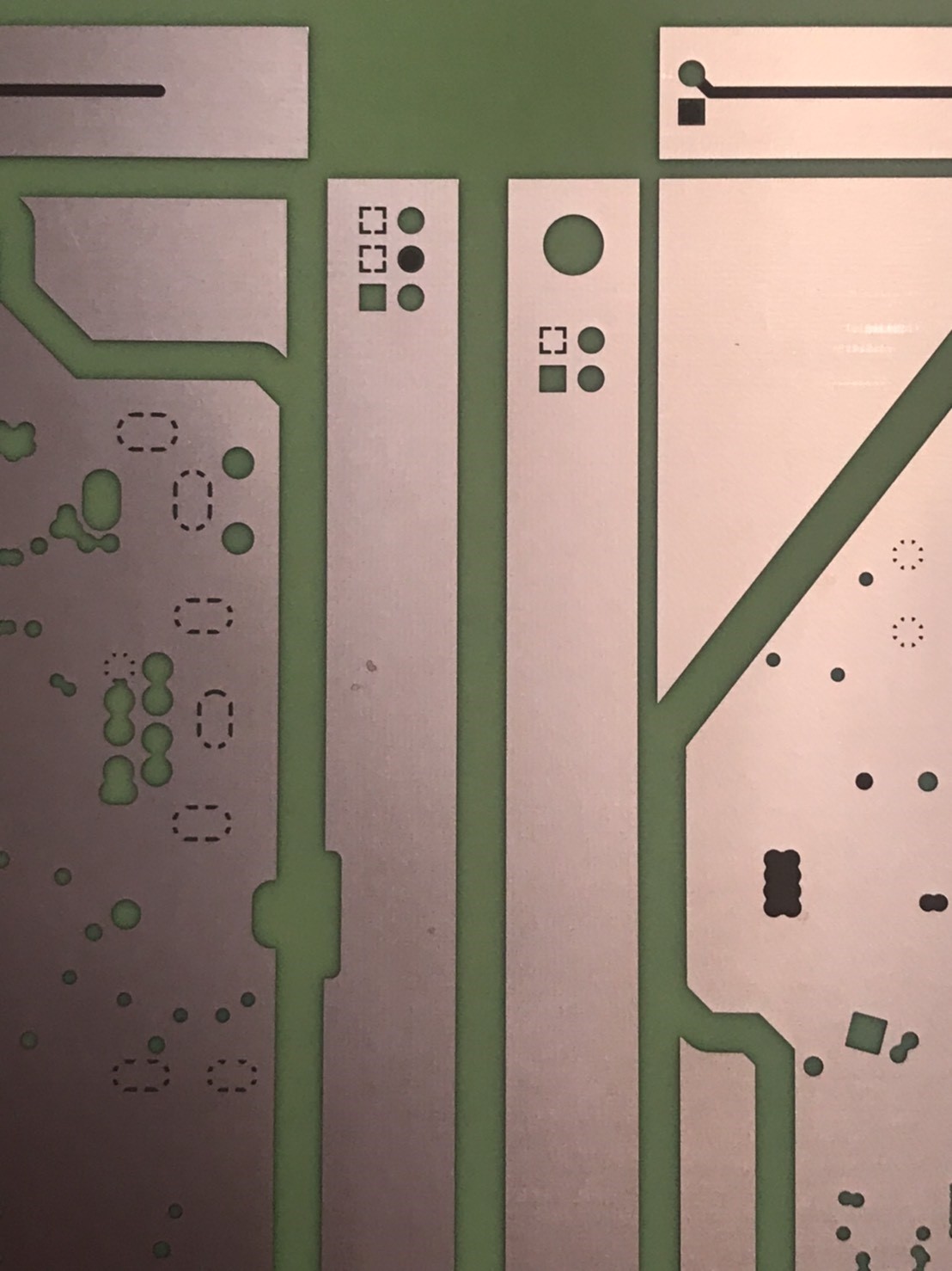
The first step is dry film lamination. To attach trace image photoresist film with base material to protect needed copper on the PCB. Second step to have UL light exposure to polymerize the film. Then the final step is to develop the trace on the PCB and to do etching with alkaline solution to remove the unprotected copper.
After the inner layer is done, of course AOI inspection is conducted to check if the trace is applied well enough.