


Common PCB Lamination Quality Issues and Improvement Methods--FAQ
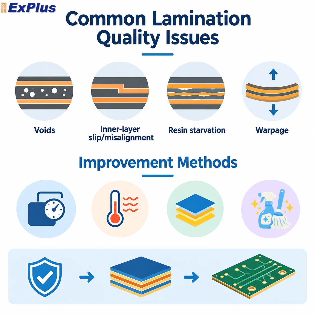
1. What are the common quality issues in PCB lamination?
Common PCB lamination defects include voids, inner-layer misalignment, resin starvation, and board warpage. These issues can affect dielectric thickness, dimensional stability, electrical performance, and overall PCB reliability.
2. What causes voids in PCB lamination, and how can they be prevented?
Voids are typically caused by trapped air or gases during the lamination process. To reduce void formation, manufacturers should improve vacuum conditions, optimize the heating profile, and ensure proper material preparation before lamination.
3. What causes inner-layer misalignment during lamination?
Inner-layer misalignment can occur when individual PCB layers shift during stacking or pressing. Proper layer registration, accurate alignment procedures, and controlled lamination conditions help minimize layer movement and maintain dimensional accuracy.
4. What is resin starvation in PCB lamination?
Resin starvation occurs when there is insufficient resin to fill the gaps between copper patterns and bond the PCB layers properly. It may result from using prepreg with insufficient resin content or from excessive resin flow during lamination.
Improvement method: Select prepreg with an appropriate resin content and precisely control the lamination heating rate and pressing conditions.
5. How can excessive resin flow be prevented?
Excessive resin flow may cause resin squeeze-out, uneven dielectric thickness, or insufficient resin remaining in critical areas. Selecting suitable prepreg materials and controlling the heating rate and lamination profile can help achieve consistent resin distribution.
6. What causes PCB warpage, and how can it be reduced?
PCB warpage refers to unwanted bending or twisting of the board. It may be associated with uneven material distribution, differences in thermal expansion, or unbalanced laminate structures.
To reduce warpage, manufacturers should optimize the PCB stack-up, maintain balanced copper distribution, and control lamination and cooling conditions.
7. Why are inner-layer cleaning and baking important before lamination?
Proper cleaning removes contaminants from inner-layer surfaces, while baking helps eliminate residual moisture. These processes help prevent bonding defects and improve lamination consistency and reliability.
8. How does lamination quality affect PCB electrical performance?
Lamination quality determines the consistency of dielectric thickness and overall board thickness. Variations in these dimensions can affect impedance control and signal integrity, particularly in high-speed and high-frequency PCB designs. Good lamination quality helps ensure stable electrical performance and long-term reliability.
9. How can PCB manufacturers improve overall lamination quality?
Manufacturers can improve lamination quality by implementing the following measures:
- Optimize vacuum levels to reduce trapped air and voids.
- Precisely control the heating rate and lamination profile.
- Select prepreg materials with suitable resin content.
- Strictly control inner-layer cleaning and baking.
- Maintain accurate layer registration and appropriate stack-up design.
- Monitor thickness uniformity, dimensional stability, and board warpage.
10. Why is lamination process control important for multilayer PCBs?
Lamination bonds multiple layers of copper and insulating materials into a unified structure. Consistent process control helps ensure reliable interlayer bonding, uniform dielectric thickness, accurate layer alignment, and stable electrical characteristics. These factors are essential for producing high-quality, reliable multilayer PCBs.