Why are PCBs green?
- Solder mask is a protective layer of polymer. It function as a mask layer by forming a protective coating on PCB. The main purpose is for preventing copper trace on PCB from contamination. Furthermore, by covering solder mask on copper trace could prevent broken trace. (Some exposed pads might risk falling out and solder mask could minimize the situation). The solder mask is moisture proof and can provide insulation, resistance, heat endurance and to maintain appearance.
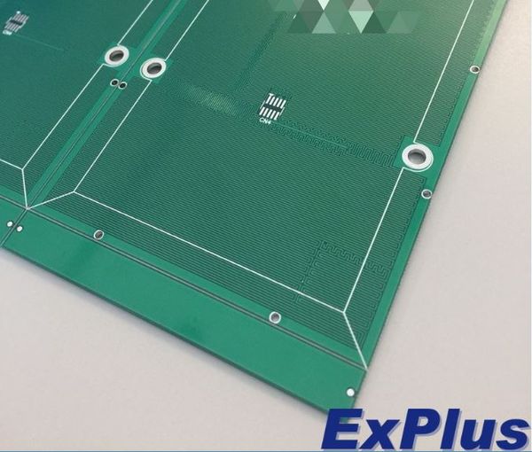
- Solder mask, also known as solder resist. Though 99% of PCB use green solder mask, there are other solder mask color available for consideration, such as red, black, blue and so on.
- The most common used PCB solder mask is made of Epoxy Liquid. It is typically applied using silkscreen techniques onto the top and bottom side of PCB, where the soldering is not required. In some occasions, the PCB manufacturers might apply inkjet printing technology.
- In general, most of PCB manufacturers would apply the lacquer on entire PCB and then put in the oven during pre-baking process and then exposure the film by using contact-exposure technology to transfer the image onto the solder mask layer.
- The process of solder mask seems fairly easy. However, if the solder mask is not applied properly during PCB manufacturing process, it might cause some quality issues, such as contamination, skip printing, copper exposure, unequal printing etc. Moreover, the thickness and displacement of solder mask could have affected the quality of tin soldering during SMT.
Maybe you would like to read more:

