

Purpose of Back drill For Printed Circuit Board
Purpose of Back drill For Printed Circuit Board
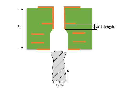
Back drillis a drill process for plated hole (via) on the PCB, the main purpose of back drill process is to reduce the length of the stub and its capacitance effect by eliminating the excess copper in the plated hole (via) on the PCB.
By eliminating the excess copper in the plated hole, the transmission characteristics of high-speed signals can be improved, further increasing the transmission speed of high-speed connectors.
Back drill can be applied to any type of circuit board where stubs cause signal integrity degradation, with minimal design and layout considerations.
Now we’re going through the advantages of Back drill below:
- Reduced deterministic jitter
- Lower bit error rate (BER)
- Less signal attenuation with improved impedance matching
- Increased channel bandwidth
- Increased data rates Reduced EMI radiation from the stubs
- Reduced excitation of resonance modes
- Reduced via-to-via crosstalk
- Aspect ratio can be neglected (in contrast to blind vias)