

Micro-section Inspection of PCB
Micro-section Inspection is a key quality analysis method used to evaluate the interlayer connections and conductor shapes of printed circuit boards. This inspection method is usually performed on the finished PCB to ensure that the conductors between each layer comply with the design requirements and production standards, or when a product defect occurs, sampling and analysis can be done at specific location to find cause of the abnormality.
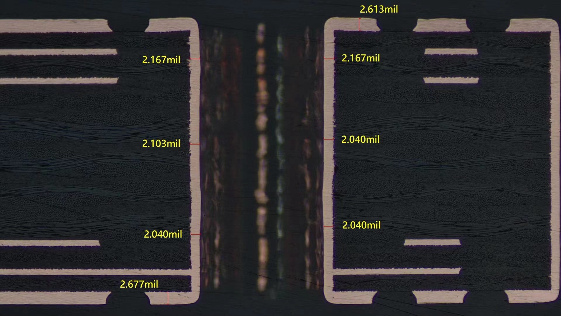
When performing micro-section inspection, a sample of a certain size is first cut from the finished PCB, and then its surface is ground to make the internal structure visible. A microscope is then used to observe and take images of micro-sections, which show the vias, conduct layers and dielectric layers of the PCB.
Through micro-section inspection, PCB manufacturers can evaluate several key factors:
- Conductor Integrity and Connections: Check whether the shape, thickness and position of the conductors are consistent with the design to ensure that the circuit connection is reliable.
- Quality of interlayer dielectric: Check the dielectric layers are even and free of cracks or air voids to prevent short circuit between conductor layers or insufficient insulation strength.
- Copper plating quality of PTH holes: Check whether the copper plating of the through holes is sufficient and evenly distributed to ensure the conductivity and reliability of the product.
Micro-section inspection is an important step in quality control during the PCB manufacturing process. It can detect potential manufacturing defects early and make timely adjustments and improvements. This not only helps improve PCB manufacturing efficiency and product reliability, but also reduces the cost and time investment in subsequent testing and repair.