- Home
- PCB


PCB Fabrication Process and Methods

- 01. Inner Layer
- 02. Lamination
- 03. Drilling
- 04. PTH & Copper Plating
- 05. Dry Film Image Transfer
- 06. Solder Mask
- 07. Surface Finish
- 08. Routing
- 09. V-Cut
- 10. Test
Make inner layer traces for those cropped material.
The Inner layer imaging is a very technical step. The board will be attached a layer of photoresist film and polymerized after apply a blast of UV light, At this point, it is ready for developing. For the development phase, the board is washed with an alkaline solution which removes the photoresist left unhardened. The unprotected copper is removed and defines the pattern. After development and etching, the inner layer will be checked if there’s any defects by automatic optical inspection (AOI).
.jpg)
Use the core material and outer layer copper foil to laminate the finished inner layer board.
The inner substrate, pre-preg and copper foil will be laid up together by its order. And then the stack-up will be placed inside the lamination machine and exposed to high pressure and temperature. Under pressure, the melted glue will bond the layers together. After the pressing is completed, the plate is moved to a cold press and then demolded. After the whole process is completed, the layers become a single board.

Use CNC drilling machine to drill holes, which for connecting conductor from layer to layer and mounting components .
Processing holes such as parts holes, fixed holes, and via holes according customer’s design, and provide positioning holes required for subsequent processes. The drilling machine is computer-controlled. The operator set up the drill program. High speed drilling ensures clean hole walls to provide a secure base for good plating on the hole walls.
Drilling is a slow process as each hole must be drilled individually. We can drill holes down to 8 mil in diameter. Drill change is fully automatic. The machine selects the correct drill to use from the drill rack, and then loads it into the drill head.
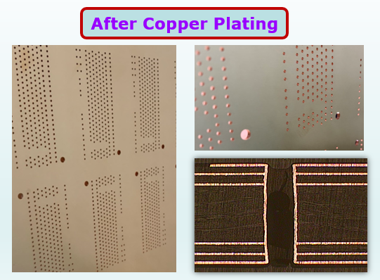
Copper plating is carried out in the hole to realize layer-to-layer wiring connection.
Removing the glue residue left on the hole wall after drilling, plate copper on the hole-wall to realize pattern connection between layers, the copper surface is thickened by electroplating to meet the customer and subsequent process requirements.
Make wire traces on the outer layer of the copper-plated board.
Cover the surface of the board with a layer of organic film that is optically active, and after exposure, transfer the pattern of the outer film to the board surface. And thicken the outer layer circuit by second electroplating.

Cover the PCB with insulating resin to protect the tracks of the outer layer from oxidation and short circuits.
Soldermask is a protective layer of liquid photo imageable lacquer applied on the top and bottom side of a PCB. The function of the soldermask is to protect the copper from oxidation, environmental influences like dust and other contaminations that may create circuit shorts in the long run.

Improve the solderability and protect the area without solder mask from oxidation, which may influence the stability.
To protect the copper solder pads on a PCB from oxidation, contamination and to enhance their solderability, they need to be protected with a Surface Finish.
ExPlus offers the following Surface Finishes:
● Hot Air Solder Levelling ( HASL / Lead-Free HASL)
● Immersion Gold (ENIG)
● Electroplated Ni/Au (Hard Gold) for Edge Connectors
● Carbon for Switch Contacts
● Organic Solderability Preservative (OSP)
● Immersion Silver

A CNC milling machine is used to form the PCB according to the required design contour.
Routing or milling is a technique performed on a CNC machine with a routing tool. Milling is used to form the contour of the PCB at the very end of the production process. For this, we use a computer-controlled milling machine. First the machine mills out any small slots or internal cut-outs. The cutter follows the path defined in the original tool file and mills around each PCB. The brush around the milling head ensures that all the dust produced is collected by the vacuum system.
A cutting line is formed on the surface of the PCB to make it easier to depanelized.
V-cut also named as V-Scoring or V-grooving, it is the final manufacturing stage of PCBs. It is cutting a “v” groove on the top and bottom of a PCB while leaving a minimum amount of material, so that a individual PCB can be easily separated from the production panel.
Conduct electrical tests and other necessary tests to ensure the quality of the circuit board.
ExPlus conducts 100% electrical tests on circuit boards before shipping to the costumer. We also provide Hipot test to meet the requirement of customers. Our PCB test systems include:
● The flying probe testers, which are suitable for testing small batches and highly complex PCBs.
● Universal grid testers, which require the use of a separate test fixture, are well suited for testing bulk-manufactured PCBs.